agosto 19, 2020 - Sony
Sony to release high-precision GNSS receiver LSIs for IoT and wearable devices
Comunicato Stampa disponibile solo in lingua originale.
Delivering the Industry’s Lowest Power Consumption*1 for Dual-Band Positioning Operation.
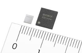
Sony Corporation announced today the upcoming release of high-precision Global Navigation Satellite System (GNSS) receiver LSIs for use in IoT and wearable devices. The new receiver LSIs boast the industry’s lowest power consumption*1 for dual-band positioning operation—only 9 mW.*2
*1: Among GNSS receiver LSIs. According to #sony research. (As of August 19, 2020, the date of this release.)
*2: For the CXD5610GF GNSS receiver LSI.
| Model names | Sample shipment date | Sample price (excluding tax) |
| CXD5610GF and CXD5610GG GNSS receiver LSIs | September 2020 | 1,000 yen |
Increasing use of IoT and wearable devices that utilize location information has resulted in growing demand for GNSS receiver LSIs. Precise positioning and reliable communications must be ensured to maintain proper operation of IoT and wearable devices, which are being used even in difficult communication environments and unstable conditions, such as multipath propagation*3 situations caused by reflection off the ground or nearby buildings or the effects of the swinging of the arms when attached to a person’s wrist. Additionally, device size constraints necessitate a compact battery, whereas satellite signal reception and positioning when using GNSS functionality typically consumes a lot of power, resulting in poor battery life.
The new LSIs support not only the conventional L1 band reception, but also L5 band reception, which is currently being expanded across GNSS constellations, thereby making them capable of dual-band positioning. Sony’s original algorithms enable stable, high-precision positioning even under the difficult conditions unique to wearable devices. Also, the use of Sony’s original high-frequency analog circuit technology and digital processing technology delivers the industry’s lowest power consumption during continuous positioning for dual-band reception operation, at only 9 mW.
The new LSIs will drive greater opportunities to develop new products and services such as smartwatches and other wearable devices that cannot use external power supplies, as well as IoT devices used for applications such as trackers. They also show promise in a wide variety of applications which require precise positioning and stable communications, such as automotive services.
*3: Signals traveling along multiple, differing pathways due to reflection and other factors, resulting in signal disturbance on the receiving end.
Main Features
■ High-precision, stable positioning via dual-band operation with the industry’s lowest power consumption
Compared with the L1 band, the new signal method used in the L5 band employs signal units that are 10 times narrower to measure the range between the GNSS satellite and receiver, improving positioning precision and amplifying the transmission power from the satellite, resulting in high-precision, high-sensitivity positioning.
Quick, accurate GNSS signal reception via Sony’s original algorithms enables positioning that is more stable than conventional products*4 even in changing reception environments, such as obstructing from buildings when on the move and acceleration of wearables due to swinging of the arms. This also leads to quick positioning time even from cold starts,*5 which require more time. Additionally, Sony’s original digital signal processing technology enables countermeasures against the performance degradation caused by radio interference from aircraft communications as well as spoofing attacks and other issues, thereby improving resistance to interference.
Low power consumption and high sensitivity are delivered by Sony’s original analog circuit technology, which enables low-voltage operation, as well as digital circuits and software algorithms that enable software processing via low clock frequencies. This innovative design keeps power consumption to only 9 mW, the lowest in the industry, when simultaneously receiving signals in both the L1 and L5 bands.
*4 For Sony’s CXD5605GF GNSS receiver LSI
*5 Positioning without the current time, current location, or satellite information.
■ Built-in memory
The new LSI’s feature built-in non-volatile memory for storing firmware, etc. This design makes it possible to update the firmware without adding externally mounted memory and contributes to a more compact design for IoT and wearable devices by saving space. It also makes it possible to complete data-processing in the products, resulting in low power consumption and improved access speed.










 Inglese
  Condividi
 Condividi via mail
  Automotive
 Sport
Sport Events
 Art&Culture
 Design
 Fashion&Beauty
 Food&Hospitality
 Tecnologia
 Nautica
 Racing
 Excellence
 Corporate
 OffBeat
 Green
Green Gift
Gift Pop
Pop Heritage
 Entertainment
 Health & Wellness